- 您现在的位置:买卖IC网 > Sheet目录2008 > MAX1240AEPA+ (Maxim Integrated Products)IC ADC 12BIT SERIAL 8-DIP
MAX1240/MAX1241
+2.7V, Low-Power,
12-Bit Serial ADCs in 8-Pin SO
2
_______________________________________________________________________________________
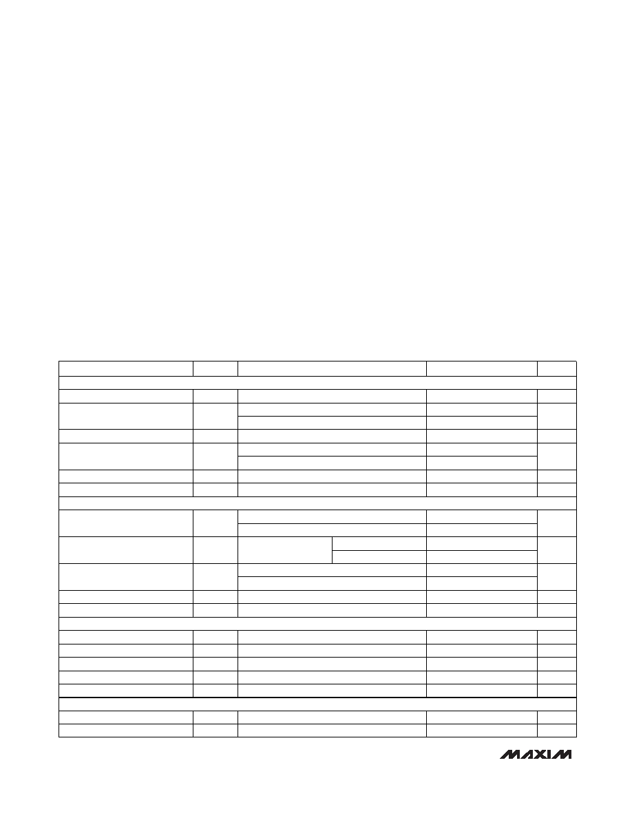
ELECTRICAL CHARACTERISTICS
(VDD = +2.7V to +3.6V (MAX1240); VDD = +2.7V to +5.25V (MAX1241); 73ksps, fSCLK = 2.1MHz (50% duty cycle); MAX1240—4.7F
capacitor at REF pin, MAX1241—external reference; VREF = 2.500V applied to REF pin; TA = TMIN to TMAX; unless otherwise noted.)
VDD to GND .............................................................-0.3V to +6V
AIN to GND................................................-0.3V to (VDD + 0.3V)
REF to GND ...............................................-0.3V to (VDD + 0.3V)
Digital Inputs to GND...............................................-0.3V to +6V
DOUT to GND............................................-0.3V to (VDD + 0.3V)
DOUT Current ..................................................................±25mA
Continuous Power Dissipation (TA = +70°C)
Plastic DIP (derate 9.09mW/°C above +70°C) ...........727mW
SO (derate 5.88mW/°C above +70°C)........................471mW
CERDIP (derate 8.00mW/°C above +70°C)................640mW
Operating Temperature Ranges
MAX1240_C_A/MAX1241_C_A .........................0°C to +70°C
MAX1240_E_ A/MAX1241_E_ A .....................-40°C to +85°C
MAX1240_MJA/MAX1241_MJA ...................-55°C to +125°C
Storage Temperature Range............................-60°C to +150°C
Lead Temperature (soldering, 10s) ................................+300°C
Soldering Temperature (reflow)
PDIP, SO .....................................................................+260°C
CDIP ...........................................................................+250°C
ABSOLUTE MAXIMUM RATINGS
Stresses beyond those listed under “Absolute Maximum Ratings” may cause permanent damage to the device. These are stress ratings only, and functional
operation of the device at these or any other conditions beyond those indicated in the operational sections of the specifications is not implied. Exposure to
absolute maximum rating conditions for extended periods may affect device reliability.
71.5
MAX124_C
Input Voltage Range
0VREF
V
Input Capacitance
Aperture Jitter
<50
ps
16
pF
MAX124_A
MAX124_B/C
Aperture Delay
tAPR
30
ns
Figure 8
Track/Hold Acquisition Time
tACQ
1.5
s
Throughput Rate
73
ksps
fSCLK = 2.1MHz
Conversion Time
PARAMETER
SYMBOL
MIN
TYP
MAX
UNITS
±0.5
±3.0
Offset Error
LSB
Differential Nonlinearity
DNL
±1
LSB
±1.0
Gain Temperature Coefficient
±0.5
±4.0
Gain Error (Note 3)
LSB
±0.5
±4.0
Resolution
12
Bits
Relative Accuracy (Note 2)
INL
±0.5
LSB
tCONV
5.5
7.5
s
Small-Signal Bandwidth
Signal-to-Noise Plus
Distortion Ratio
SINAD
70
dB
2.25
MHz
Full-Power Bandwidth
Total Harmonic Distortion
THD
-80
dB
1.0
-3dB rolloff
MHz
CONDITIONS
Spurious-Free Dynamic Range
ppm/°C
No missing codes over temperature
MAX124_B/C
±0.25
SFDR
MAX124_A/B
80
Up to the 5th harmonic
dB
MAX124_A/B
MAX124_A
MAX124_A/B
MAX124_C
-88
MAX124_C
88
ANALOG INPUT
CONVERSION RATE
DYNAMIC SPECIFICATIONS (10kHz sine-wave input, 0V to 2.500Vp-p, 73ksps, fSCLK = 2.1MHz)
DC ACCURACY (Note 1)
发布紧急采购,3分钟左右您将得到回复。
相关PDF资料
MAX1245BCPP
IC ADC SRL 12BIT 2.375V 20-DIP
MAX1249AEPE+
IC ADC 10BIT SERIAL 16-DIP
MAX1279AETC+
IC ADC 12BIT 1.5MSPS 12-TQFN
MAX1285BESA+T
IC ADC 12BIT 300KSPS 8-SOIC
MAX1302BEUG+
IC ADC 16BIT SRL 115KSPS 24TSSOP
MAX1303BEUP+
IC ADC 16BIT MULT RANGE 20TSSOP
MAX1308ECM+T
IC ADC 12BIT 8CH 4MSPS 48LQFP
MAX1320ECM+T
IC ADC 14BIT 8CH 2MSPS 48LQFP
相关代理商/技术参数
MAX1240AESA
功能描述:模数转换器 - ADC RoHS:否 制造商:Texas Instruments 通道数量:2 结构:Sigma-Delta 转换速率:125 SPs to 8 KSPs 分辨率:24 bit 输入类型:Differential 信噪比:107 dB 接口类型:SPI 工作电源电压:1.7 V to 3.6 V, 2.7 V to 5.25 V 最大工作温度:+ 85 C 安装风格:SMD/SMT 封装 / 箱体:VQFN-32
MAX1240AESA/V+
功能描述:模数转换器 - ADC 12-Bit 73ksps 3.6V Precision ADC RoHS:否 制造商:Texas Instruments 通道数量:2 结构:Sigma-Delta 转换速率:125 SPs to 8 KSPs 分辨率:24 bit 输入类型:Differential 信噪比:107 dB 接口类型:SPI 工作电源电压:1.7 V to 3.6 V, 2.7 V to 5.25 V 最大工作温度:+ 85 C 安装风格:SMD/SMT 封装 / 箱体:VQFN-32
MAX1240AESA/V+T
功能描述:模数转换器 - ADC 12-Bit 73ksps 3.6V Precision ADC RoHS:否 制造商:Texas Instruments 通道数量:2 结构:Sigma-Delta 转换速率:125 SPs to 8 KSPs 分辨率:24 bit 输入类型:Differential 信噪比:107 dB 接口类型:SPI 工作电源电压:1.7 V to 3.6 V, 2.7 V to 5.25 V 最大工作温度:+ 85 C 安装风格:SMD/SMT 封装 / 箱体:VQFN-32
MAX1240AESA+
功能描述:模数转换器 - ADC 12-Bit 73ksps 3.6V Precision ADC RoHS:否 制造商:Texas Instruments 通道数量:2 结构:Sigma-Delta 转换速率:125 SPs to 8 KSPs 分辨率:24 bit 输入类型:Differential 信噪比:107 dB 接口类型:SPI 工作电源电压:1.7 V to 3.6 V, 2.7 V to 5.25 V 最大工作温度:+ 85 C 安装风格:SMD/SMT 封装 / 箱体:VQFN-32
MAX1240AESA+T
功能描述:模数转换器 - ADC 12-Bit 73ksps 3.6V Precision ADC RoHS:否 制造商:Texas Instruments 通道数量:2 结构:Sigma-Delta 转换速率:125 SPs to 8 KSPs 分辨率:24 bit 输入类型:Differential 信噪比:107 dB 接口类型:SPI 工作电源电压:1.7 V to 3.6 V, 2.7 V to 5.25 V 最大工作温度:+ 85 C 安装风格:SMD/SMT 封装 / 箱体:VQFN-32
MAX1240AESA-T
功能描述:模数转换器 - ADC RoHS:否 制造商:Texas Instruments 通道数量:2 结构:Sigma-Delta 转换速率:125 SPs to 8 KSPs 分辨率:24 bit 输入类型:Differential 信噪比:107 dB 接口类型:SPI 工作电源电压:1.7 V to 3.6 V, 2.7 V to 5.25 V 最大工作温度:+ 85 C 安装风格:SMD/SMT 封装 / 箱体:VQFN-32
MAX1240AMJA
功能描述:模数转换器 - ADC
RoHS:否 制造商:Texas Instruments 通道数量:2 结构:Sigma-Delta 转换速率:125 SPs to 8 KSPs 分辨率:24 bit 输入类型:Differential 信噪比:107 dB 接口类型:SPI 工作电源电压:1.7 V to 3.6 V, 2.7 V to 5.25 V 最大工作温度:+ 85 C 安装风格:SMD/SMT 封装 / 箱体:VQFN-32
MAX1240BCPA
功能描述:模数转换器 - ADC Integrated Circuits (ICs) RoHS:否 制造商:Texas Instruments 通道数量:2 结构:Sigma-Delta 转换速率:125 SPs to 8 KSPs 分辨率:24 bit 输入类型:Differential 信噪比:107 dB 接口类型:SPI 工作电源电压:1.7 V to 3.6 V, 2.7 V to 5.25 V 最大工作温度:+ 85 C 安装风格:SMD/SMT 封装 / 箱体:VQFN-32